NVLink and NVSwitch Explained: GPU Interconnect for AI at Scale
Discover how high-speed GPU fabric technology eliminates interconnect bottlenecks in large-scale machine learning and enterprise compute.
CryptoMine Editorial · August 1, 2026 · 7 min read

As artificial intelligence models grow exponentially in parameter size, hardware requirements have shifted from single-accelerator performance to system-level interconnect scalability. Modern Large Language Models (LLMs) and complex High Performance Computing (HPC) simulations demand massive VRAM bandwidth and compute throughput that exceed the capacity of a single graphics processing unit. To train and run inference on multi-billion parameter models effectively, enterprises must link multiple GPUs so they operate as a single, cohesive system. In this technical guide, having NVLink NVSwitch explained provides system architects, procurement leads, and machine learning engineers with the foundation needed to evaluate high-speed GPU interconnect fabrics for enterprise AI infrastructure.
Standard PCIe expansion slots, while reliable for traditional workstation and server applications, create severe data transfer bottlenecks when scaling distributed tensor parallelism. When processing large batch sizes across multiple GPUs, data transfer speeds over standard system buses become the primary bottleneck. NVIDIA developed NVLink and NVSwitch to bypass these architectural limitations, providing direct GPU-to-GPU communications with bandwidth throughput multi-fold higher than traditional PCIe lanes.
The PCIe Bottleneck vs. High-Bandwidth GPU Interconnects
In traditional x86 or ARM server architectures, graphics processors communicate with each other across the host system Peripheral Component Interconnect Express (PCIe) bus, managed by the host CPU root complex. PCIe Gen 5 offers up to 64 GB/s of unidirectional bandwidth (128 GB/s bidirectional) across a standard x16 lane configuration. While this bandwidth is sufficient for lightweight inference tasks or single-GPU workstation workloads, it falls short when executing large-scale distributed deep learning models.
In distributed deep learning workflows—such as tensor parallel model execution—GPUs must continuously exchange intermediate activation layers and weight updates during forward and backward passes. Routing these massive data payloads through host RAM and CPU root complexes introduces severe latency overhead, high CPU utilization, and system bus congestion.
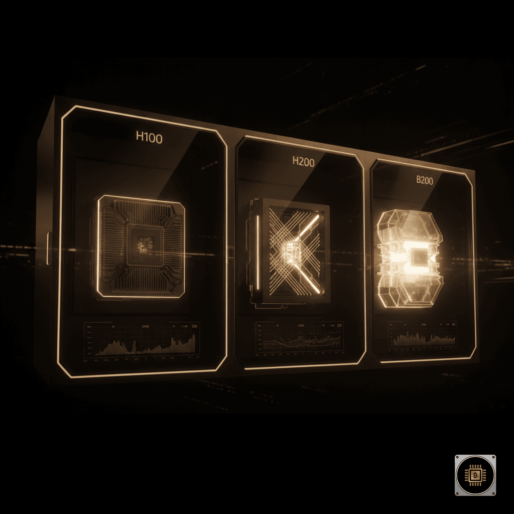
High-bandwidth interconnects solve this problem by establishing direct, dedicated physical links between GPU modules. By enabling direct access to adjacent High-Bandwidth Memory (HBM) banks without CPU intervention, high-speed interconnects allow distributed clusters to maintain maximum TFLOPS utilization across all installed accelerators. For enterprise deployments requiring high-density compute, deploying accelerators such as the NVIDIA H100 80GB or the high-capacity NVIDIA H200 allows organizations to take full advantage of these ultra-fast interconnect architectures.
High-Performance GPU Interconnects: NVLink and NVSwitch Explained
To understand how modern AI clusters achieve near-linear performance scaling across dozens or thousands of compute engines, it is essential to examine the distinct roles played by NVLink hardware connections and NVSwitch fabric processors.
NVLink: Direct High-Speed Point-to-Point Links
NVLink is a high-speed, point-to-point interconnect protocol designed specifically for direct GPU-to-GPU data transmission. Rather than converting packet protocols to pass through system host memory, NVLink transfers data using an optimized signal protocol directly between high-performance processors.
Key technological features of NVLink include:
- High Bidirectional Bandwidth: Generations of NVLink have progressively increased total bandwidth per card. Fourth-generation NVLink, found in Hopper architecture GPUs, delivers up to 900 GB/s of total bidirectional bandwidth per GPU—more than seven times the bandwidth of PCIe Gen 5.
- Direct HBM Access: NVLink enables remote memory access across GPUs with minimal latency. Accelerators can read and write directly to each other's VRAM pool using hardware-based Remote Direct Memory Access (RDMA) primitives.
- Unified Memory Space: Through software frameworks like CUDA, software engineers can address VRAM across connected GPUs as a contiguous memory pool, simplifying programming models for complex ML architectures.
- Reduced Host Overhead: By bypassing host CPU memory registers entirely, NVLink frees up host CPU cores and system RAM bandwidth for general input/output and data preprocessing tasks.
NVSwitch: Non-Blocking Enterprise Fabric Switching
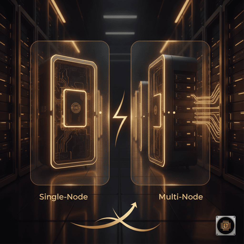
While NVLink establishes fast point-to-point paths between pairs or small clusters of GPUs, pure point-to-point connections become physically impractical as GPU density increases. Connecting eight GPUs in a fully meshed point-to-point network would require an unmanageable number of physical links per accelerator.
This is where NVSwitch becomes essential. NVSwitch is a dedicated high-bandwidth crossbar switch chip integrated directly into the server baseboard or external switch fabric trays. Instead of running discrete point-to-point traces between every GPU, every GPU connects directly to the NVSwitch ICs.
The key capabilities of NVSwitch include:
- All-to-All Non-Blocking Communication: NVSwitch allows every connected GPU in a multi-GPU system to communicate with any other GPU simultaneously at full NVLink speed without throughput degradation.
- Multi-GPU Node Scaling: Within an 8-GPU SXM baseboard enterprise system, multiple NVSwitch chips route inter-GPU traffic seamlessly across all eight nodes, creating a single logical compute system with high aggregate interconnect bandwidth.
- Rack-Scale Expansion: External NVSwitch trays allow organizations to extend the NVLink fabric beyond a single chassis, linking multiple physical servers into a unified NVLink network domain comprising hundreds of GPUs.
Impact on Modern AI Workloads and Model Scaling
The combination of NVLink and NVSwitch architectures directly dictates how effectively enterprise data centers can scale demanding AI and HPC workloads.
Tensor Parallelism and Model Sharding
State-of-the-art LLMs containing hundreds of billions of parameters cannot fit into the VRAM of a single accelerator card. To run these models, machine learning teams use model parallelism, sharding model weights across multiple GPUs. Tensor parallelism breaks individual neural network layers across separate processors, requiring synchronization at every single layer execution step.
Without high-speed interconnects like NVLink and NVSwitch, the communication latency between layers dominates total execution time, causing GPU compute cores to sit idle waiting for data transfers. NVSwitch-enabled nodes eliminate this execution bottleneck, enabling linear performance scaling during LLM training and ultra-low latency real-time inference.
Distributed HPC Simulations and Rendering
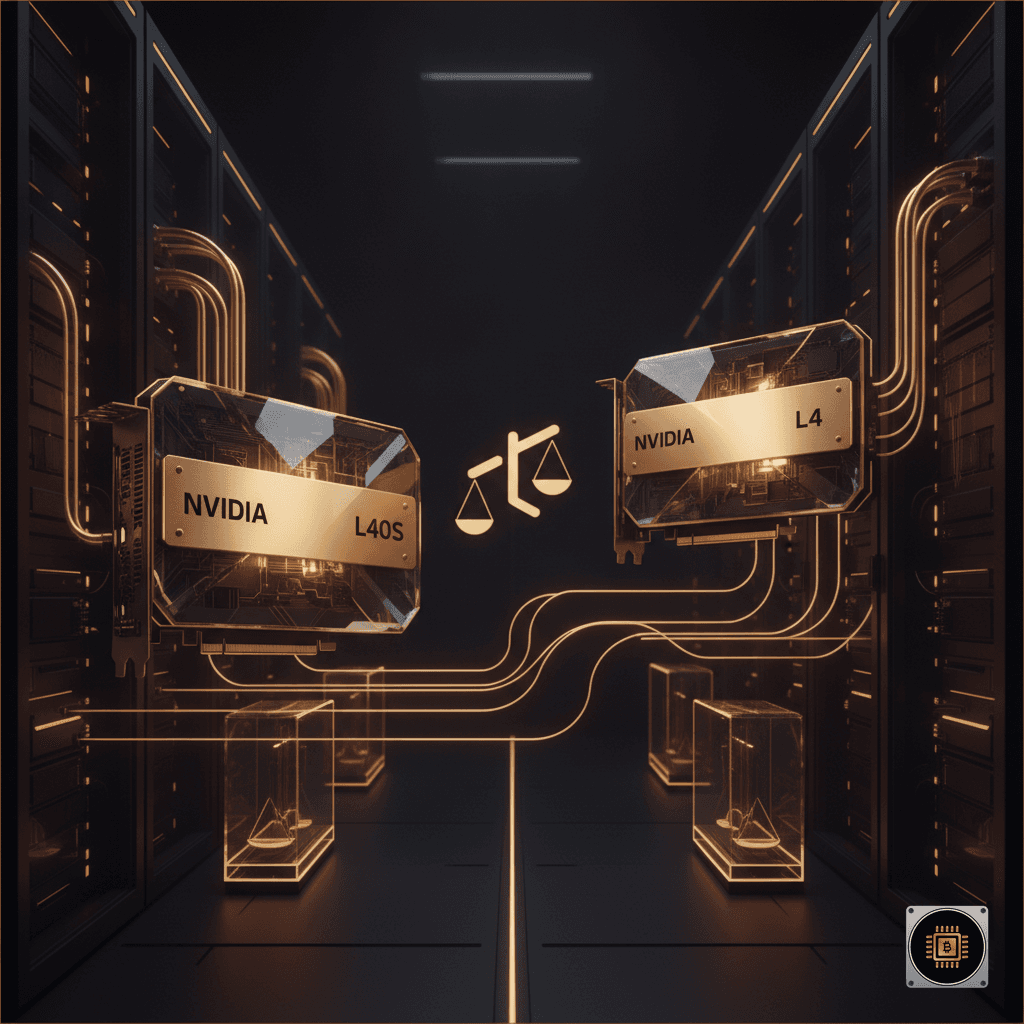
In computational fluid dynamics, molecular dynamics, and enterprise rendering pipelines, large datasets must be processed concurrently. While data-parallel tasks with low inter-node communication can run effectively on standard enterprise graphics cards or universal data center cards like the NVIDIA L40S, heavily coupled HPC simulations benefit immensely from pooled VRAM and rapid all-reduce synchronization provided by NVLink topologies.
Hardware Configurations and Procurement Considerations for AI Infrastructure
When selecting infrastructure for data center deployment, enterprise procurement managers must evaluate several technical factors regarding interconnect options:
- Form Factor Selection: SXM form factor boards feature fully integrated NVLink and NVSwitch routing directly on the substrate, providing the highest possible interconnect bandwidth. Conversely, standard PCIe form factor accelerator cards typically rely on discrete physical NVLink bridges between adjacent cards or rely entirely on PCIe bus communication.
- Server Platform Compatibility: Enterprise multi-GPU deployments demand robust chassis designs built to support high power draw and dense cooling requirements. High-density server platforms such as the Supermicro AS-4125GS GPU Server, alongside standard rack enterprise systems like the Dell PowerEdge R760 or HPE ProLiant DL380 Gen11, provide the structural, electrical, and thermal foundation required for heavy enterprise AI hardware configurations.
- Thermal Management and Power Infrastructure: High-density NVSwitch systems draw substantial power and require carefully planned airflow or liquid cooling solutions within the server room to maintain thermal stability under peak operational throughput.
Maximizing AI Performance with CryptoMine
Selecting the appropriate GPU interconnect topology is a critical decision that dictates system throughput, training efficiency, and long-term TCO for modern data centers. Having NVLink NVSwitch explained in detail enables enterprise IT leaders, HPC researchers, and hardware architects to design balanced compute systems that prevent operational bottlenecks.
CryptoMine is a global enterprise supplier of premium AI servers, data-center GPUs, and professional workstation hardware based in the UAE. Whether your organization is deploying multi-node SXM clusters for LLM pre-training or configuring enterprise rack servers for scalable inference, CryptoMine provides worldwide delivery, expert procurement guidance, and competitive lead times for cutting-edge compute infrastructure. Explore our full range of enterprise compute solutions in our servers section or consult with our technical specialists to optimize your next infrastructure deployment.
FAQ
What is the main difference between NVLink and NVSwitch? NVLink is the high-speed point-to-point protocol and physical interface that enables direct GPU-to-GPU data transmission. NVSwitch is an enterprise physical switch chip that connects multiple NVLink channels together, enabling all-to-all, full-bandwidth communication across multiple GPUs without routing bottlenecks.
Can standard PCIe GPU cards utilize NVSwitch functionality? NVSwitch hardware integration is typically reserved for SXM-based data center architectures and specialized enterprise board configurations where multiple GPU modules are mounted directly onto a dedicated baseboard containing NVSwitch chips. Standard PCIe cards utilize host PCIe lanes or physical two-way NVLink bridges where hardware support exists.
How does NVLink improve LLM training speed compared to standard PCIe? During distributed LLM training, models use tensor parallelism which requires frequent, low-latency communication across GPU memory pools. NVLink provides up to 900 GB/s or more of bidirectional bandwidth per GPU—far exceeding the throughput of PCIe Gen 5—reducing latency, eliminating CPU overhead, and keeping compute cores running at maximum efficiency.
Do all enterprise AI workloads require NVSwitch fabrics? No. Workloads that can be easily parallelized across independent datasets without frequent inter-GPU synchronization—such as computer vision inference, embarrassingly parallel tasks, or rendering workloads—can perform efficiently on PCIe-based configurations without requiring full NVSwitch topology.

CryptoMine Editorial
Hardware specialists at CryptoMine — helping businesses choose, configure and deploy AI servers, data-center GPUs and workstation hardware.